
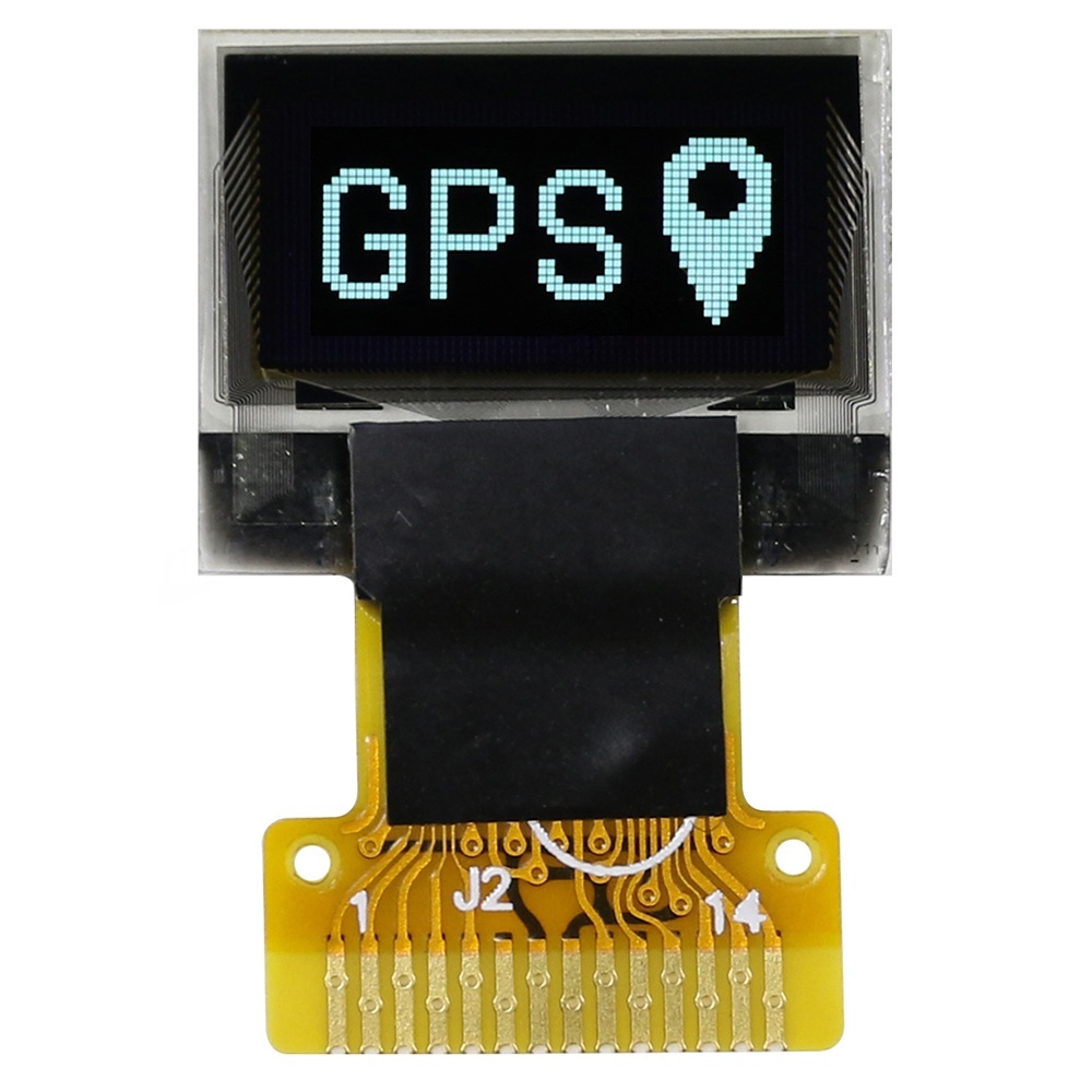
OLED Display, 0.49" 64x32 OLED Micro Display Module
►Micro OLED, OLED Micro Display
►Type: Graphic
►Structure: COG
►Size: 0.49" OLED
►64x32 Dot Matrix OLED
►IC:SSD1306
►3V Power supply
►1/32 duty
►Interface: I2C
►Display Color: White / Yellow
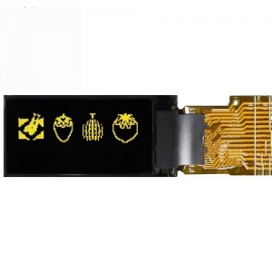
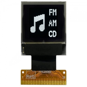
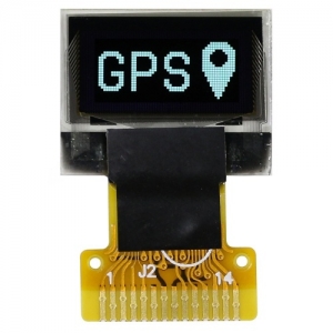
►Suitable for Wearable Device
0.49-inch micro OLED display module with a resolution of 64x32 dots. It has module dimensions of 14.5×11.6×1.26 mm and an active area size of 11.18×5.58 mm (Diagonal: 0.49"). The micro OLED display is equipped with a built-in SSD1306 IC, supporting the I2C interface. The module operates with a logic voltage of 3V and a duty cycle of 1/32. Additionally, the module supports an internal charge pump supply and external VCC supply. The OLED micro display, also referred to as a micro OLED screen, boasts a high contrast ratio of 10,000:1.
Featuring a COG (Chip-on-Glass) structure OLED display, this micro display module is ultra-thin and eliminates the need for a backlight (self-emitting). It is lightweight and consumes low power, making it ideal for various applications. The module can operate in temperatures ranging from -40℃ to +80℃, with storage temperatures ranging from -40℃ to +85℃. This small-sized 0.49-inch OLED module is well-suited for wearable devices, MP3 players, portable devices, personal care appliances, voice recorder pens, health devices, and more.
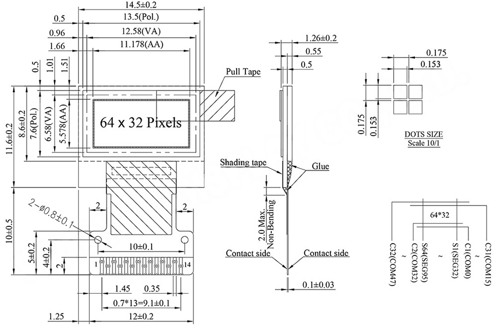
Interface Pin Function
| No. | Symbol | Function |
|---|---|---|
| 1 | C2N | C2P/C2N – Pin for charge pump capacitor; Connect to each other with a capacitor. C1P/C1N – Pin for charge pump capacitor; Connect to each other with a capacitor |
| 2 | C2P | |
| 3 | C1P | |
| 4 | C1N | |
| 5 | VBAT | This is the power supply pin for the internal buffer of the DC/DC voltage converter. It must be connected to external source when the converter is used. It should be connected to VDD or kept float when the converter is not used. |
| 6 | NC | No connection. |
| 7 | VSS | This is a ground pin. |
| 8 | VDD | Power supply pin for core logic operation. |
| 9 | RES# | This pin is reset signal input. When the pin is low, initialization of the chip is executed. Keep this pin HIGH (i.e. connect to VDD) during normal operation. |
| 10 | SCL | The serial clock input |
| 11 | SDA | The serial data input/output |
| 12 | IREF | This is segment output current reference pin. When external IREF is used, a resistor should be connected between this pin and Vss to maintain the IREF current at a maximum of 30uA. When internal IREF is used, this pin should be kept NC. |
| 13 | VCOMH | The pin for COM signal deselected voltage level. A capacitor should be connected between this pin and VSS. |
| 14 | VCC | This is the most positive voltage supply pin. When charge pump is enabled, a capacitor should be connected between this pin and VSS. |
 0.91 inch 128x32 OLED Display
 0.66-Inch OLED Display
 OLED Display, 0.49" 64x32