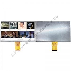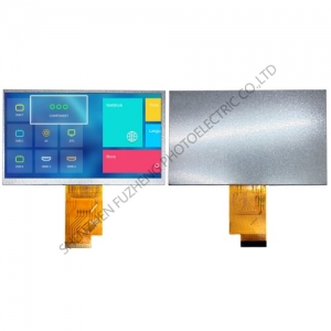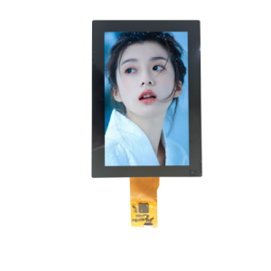
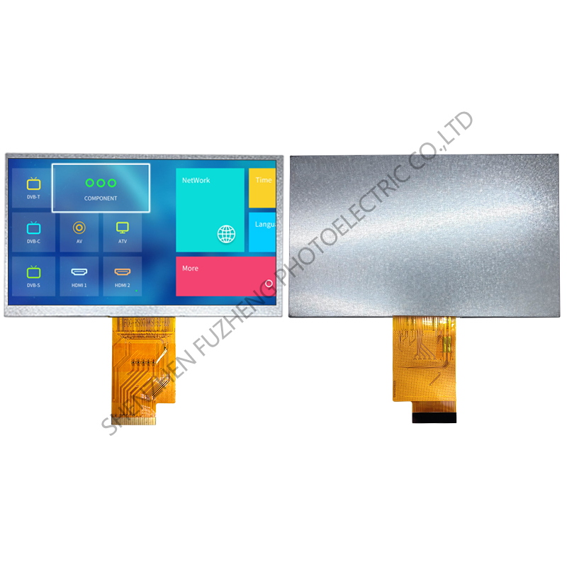
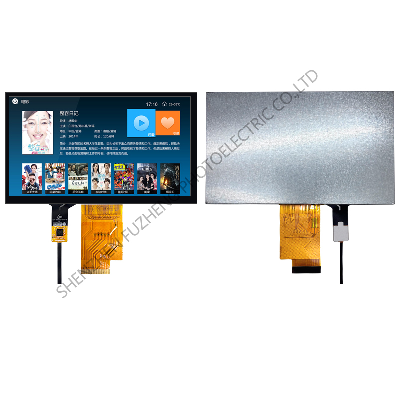
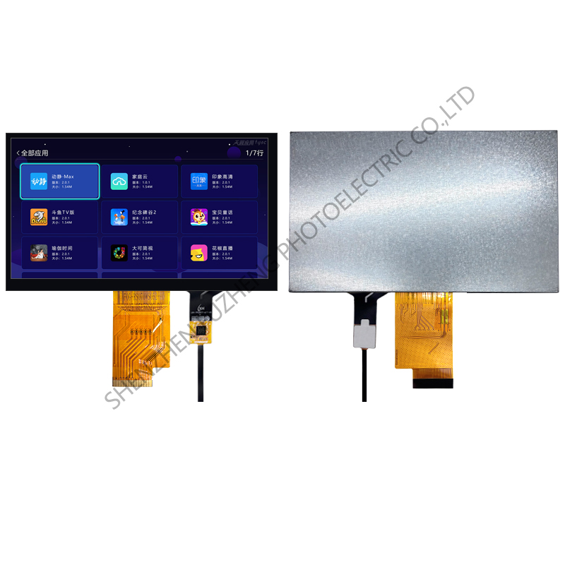
7 inch LVDS TFT Display 1024*600
| Item | Contents | Unit |
| Model | FZ7001L40 | |
| LCD Type | TFT | / |
| Viewing Direction | ALL | O' Clock |
| Size | 7 inch | inch |
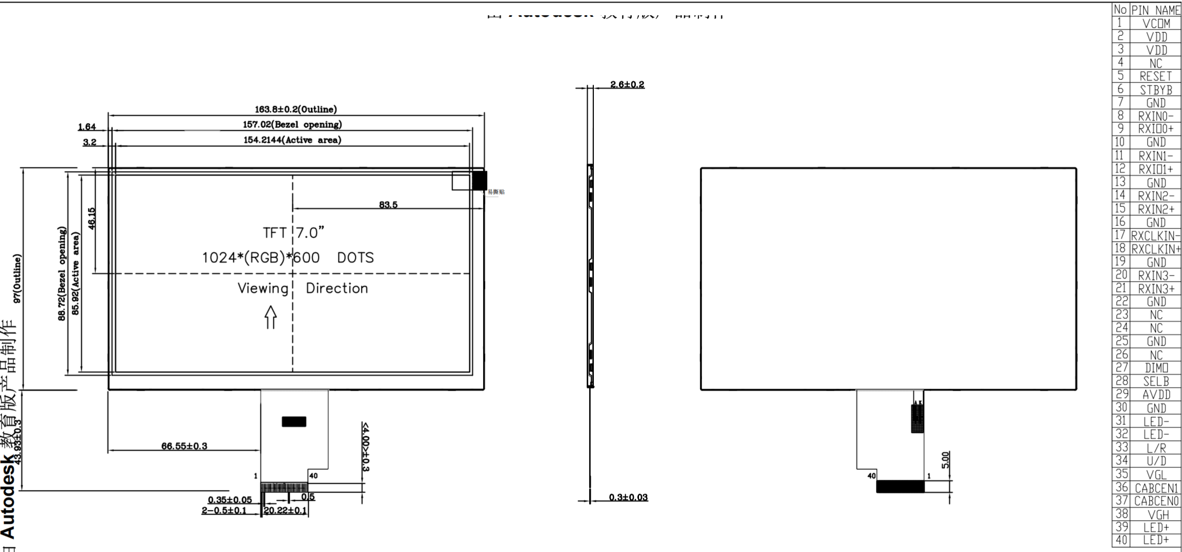
| Module Outline (W x HxD) | 165(H) ×100(V) × 3.5(T) | mm |
| Active Area (WxH) | 154.2144(H) *85.92(V) | mm |
| Resolution (pixels) | 1024*600 | / |
| Interface Type | LVDS | / |
| Input Voltage | 3.3 | V |
| Luminance | 260 | cd/m2 |
| Backlight Type And Color: | 3*6 chips white LEDS | |
| Controller IC: | HX8282/HX8696 | |
| Touch Type: | CTP (capacitive touch panel) | |
| LED Life span: | 25000 | hour |
| Operating Temperature Range: | -20 -- 70 °C | |
| Storage Temperature Range: | -30 -- 80 °C |
Electrical Specifications
Parameter | Symbol | Values | Unit | Remark | ||
Min. | Typ. | Max. | ||||
Digital supply voltage | VDD | 3 | 3.3 | 3.6 | V | |
Analog supply voltage | AVDD | - | 10.0 | - | V | |
TFT Gate ON Voltage | VGH | - | 18 | - | V | |
TFT Gate OFF Voltage | VGL | - | -6 | - | V | |
TFT Common Electrode Voltage | VCOM | 3.1 | 3.2 | -3.3 | V | |
Notes :
1. VGH is TFT Gate operating voltage.
2. VGL is TFT Gate operating voltage. The low voltage level of VGL signal must be
fluctuates with same phase as Vcom.
3. Vcom must be adjusted to optimize display quality, as Crosstalk and Contrast Ratio etc..
4. The value is just the reference value. The customer can optimize the setting value by the
different D-IC
Current Consumption
Item | Symbol | Values | Unit | Remark | ||
Min. | Typ. | Max. | ||||
Current for Driver
| IGH | - | 0.50 | 10 | mA | |
IGL | - | 0.50 | 10 | mA | ||
IVDD | - | 35 | 140 | mA | ||
IAVDD | - | 35 | 70 | mA | ||
Backlight Charac Teristics
Item | Symbol | Min | Typ | Max | Unit | Condition |
Forward voltage | Vf | - | 9.0 | - | V | If=120mA |
Luminance | Lv | - | 260 | - | cd/m2 | If=120mA |
Number of LED | -- | 18 | Piece | -- | ||
Connection mode | P | 3chips serial *6 | -- | -- | ||
Interface PIN Connections
LCM-PIN
Symbol | Function | |
1 | VCOM | Common Voltage |
2-3 | VDD | Power ground |
4 | NC | NC |
5 | RESET | Globle reset pin |
6 | U/D | Vertical inversion |
7 | L/R | Horizontal inversion |
8 | STBYB | Standby mode,Normally pulled high STBYB=”1”,normal operation STBYB=”0”,timing controller,source driver will turn off,all output are High-Z |
9 | GND | Ground |
10 | RXCLKIN- | -LVDS differential clock input |
11 | RXCLKIN+ | +LVDS differential clock input |
12 | GND | Ground |
13 | RXIN0- | -LVDS differential data input |
14 | RXIN0+ | +LVDS differential data input |
15 | GND | Ground |
16 | RXIN1- | -LVDS differential data input |
17 | RXIN1+ | +LVDS differential data input |
18 | GND | Ground |
19 | RXIN2- | -LVDS differential data input |
20 | RXIN2+ | +LVDS differential data input |
21 | GND | Ground |
22 | RXIN3- | -LVDS differential data input |
23 | RXIN3+ | +LVDS differential data input |
24 | GND | Ground |
25 | SELB | 6bit/8bit mode select |
26 | GND | Ground |
27 | AVDD | Power for Anglog Circuit |
28 | GND | Ground |
29 | VGH | Gete ON Voltage |
30-31 | NC | NC |
32 | VGL | Gete OFF Voltage |
33 | GND | Ground |
34 | NC | NC |
35-36 | LED- | LED Cathode |
37-38 | NC | NC |
39-40 | LED+ | LED Anode |
TP-PIN
1 | RST | Touch Reset Signal |
2 | VDD | Touch Power supply |
3 | GND | Ground |
4 | INT | Touch Interrupt |
5 | SDA | ouch IIC Data signal |
6 | SCA | Touch IIC Clock signal |
Prepare a product inquiry
Send the model or page link together with the following requirements so the team can check the relevant details:
- Display size, resolution and interface
- Module dimensions, connector and mounting constraints
- Touch requirements and operating environment
- Sample quantity, production volume and schedule
Where should I confirm specifications?
Use the specifications on the selected product page. Ask the team for the current datasheet and confirm any missing values before selection or ordering.
How do I request pricing and availability?
Include the model, quantity and delivery destination in your inquiry. Pricing, availability and compatibility should be confirmed for your specific request.